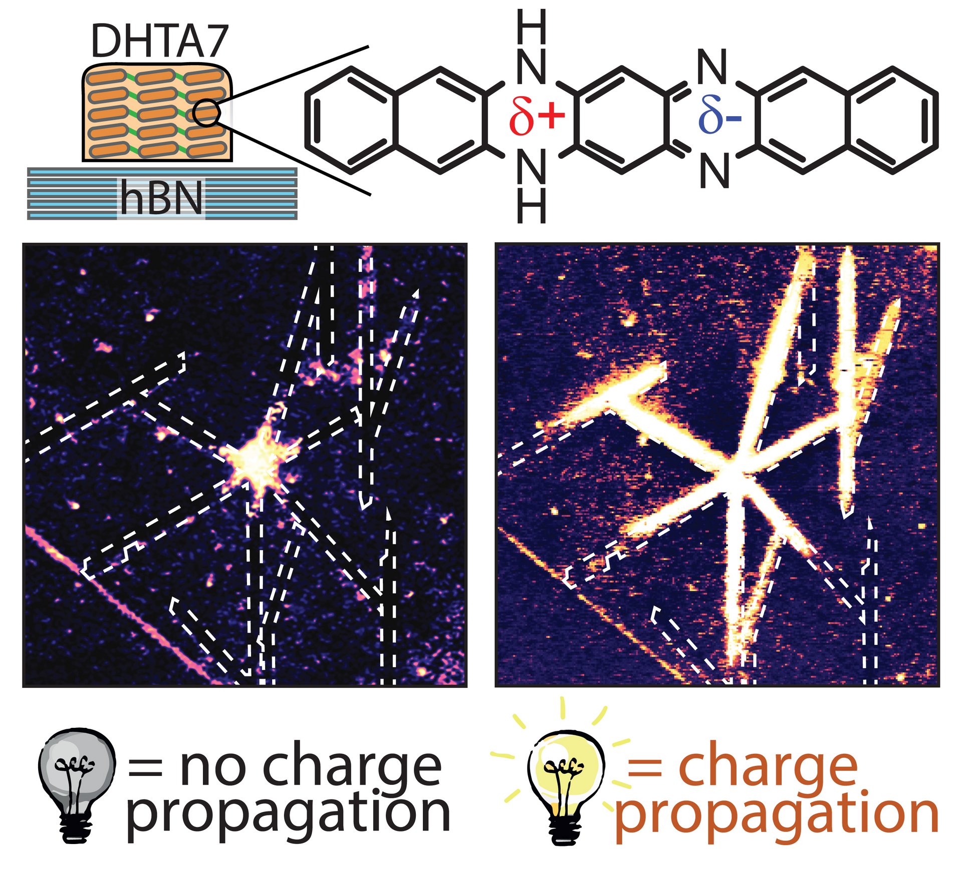
Introducing organic semiconductors as additional building blocks into heterostructures of 2D materials widens the horizon of their applications. Organic molecules can form self-assembled and self-aligned crystalline nanostructures on 2D materials, resulting in well-defined interfaces that preserve intrinsic properties of both constituents. Thus, organic molecules add unique capabilities to van der Waals heterostructures that have no analogues in inorganic matter. This study explores light-assisted charge propagation in organic semiconductor networks of quasi-1D needlelike crystallites, epitaxially grown on insulating hexagonal boron nitride. Electrostatic force microscopy is employed to demonstrate that upon external illumination it is possible to change the conductivity of organic crystallites by more than two orders of magnitude. Furthermore, by exploiting the highly anisotropic optical properties of the organic nanoneedles, a selective charge propagation along the crystallites is triggered that matches the orientation of the molecular backbones with the incident light’s polarization direction. These results demonstrate the possibility to use a “light-gate” to switch on the conductivity of organic nanostructures and even to guide the charge propagation along desired directions in self-assembled crystallite networks.
Link to the article:https://onlinelibrary.wiley.com/doi/abs/10.1002/adfm.201903816