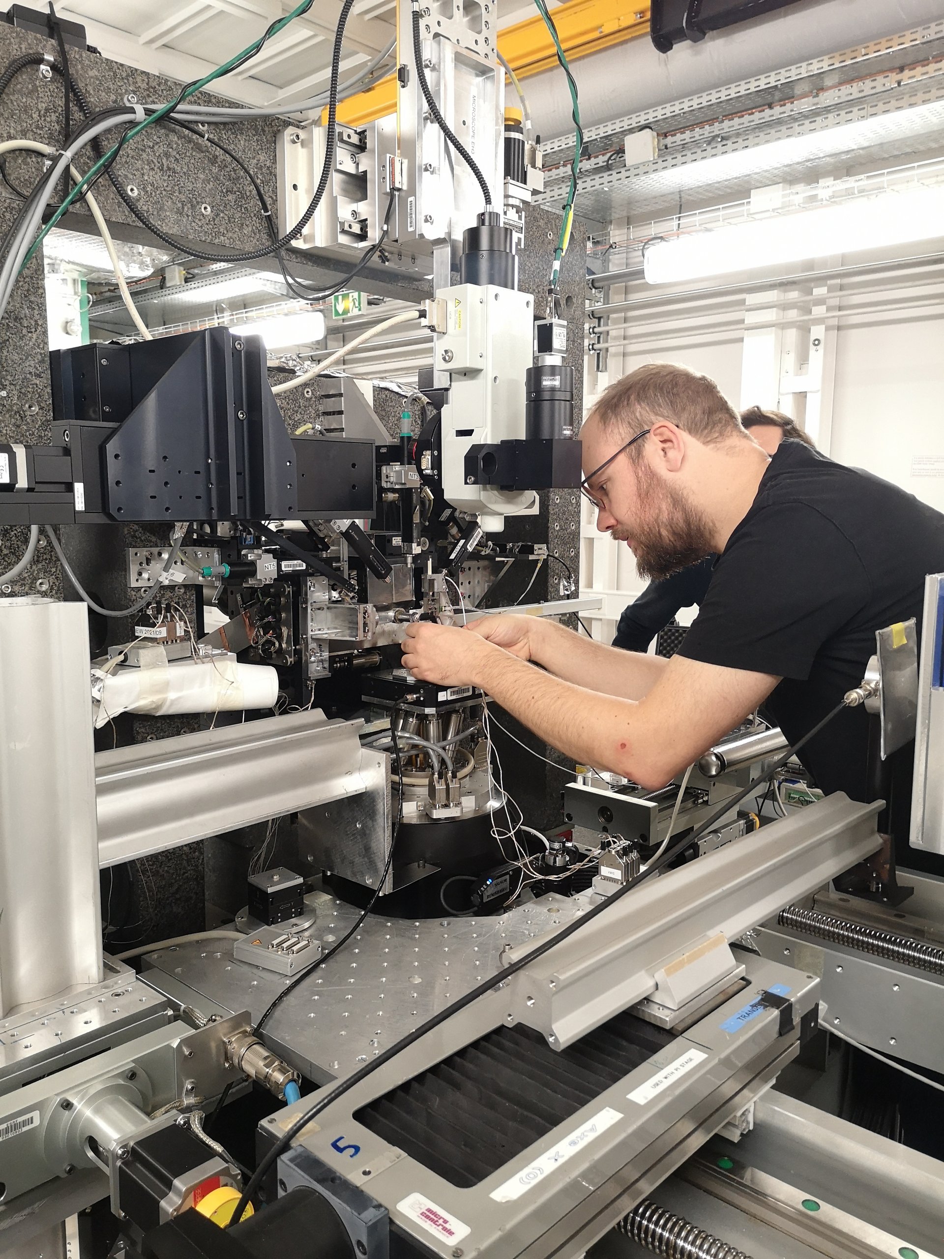
In practical applications, contact between engineering materials rarely occurs across perfectly smooth surfaces; instead, it forms along microscopic roughness peaks, known as asperities. At these tiny contact points, extreme deformation gradients and localised stress concentrations arise, which can compromise mechanical integrity and lead to failure. A team at TU Leoben has now, for the first time, experimentally quantified the stress concentrations on both sides of a single asperity under realistic contact conditions, thereby validating fundamental assumptions of contact mechanics.
Collaboration with a Major Research Facility in Grenoble
Under the leadership of Dr. Michael Meindlhumer of the Department of Materials Science and the Chair of Materials Physics, the team has shown how interfaces in a multilayered material architecture govern the development of stress concentrations and influence local deformation. To capture the complex material response under multiaxial stress concentrations, the researchers conducted two highly specialised in situ deformation experiments at the ID13 Nanofocus Beamline of the European Synchrotron Radiation Facility (ESRF) in Grenoble. Thanks to nanometre-precise X‑ray focusing, they were able to visualise the stress distribution directly at the contact site at nanometre scale and on both sides of the asperity.
Preventing Material Failure
The results show that a multilayer composite with nanoscale, ductile interlayers can dissipate up to one-third of the elastic energy stored in the material through plastic deformation. This controlled energy dissipation mitigates local stress peaks and thus prevents catastrophic failure. It is particularly noteworthy that complementary micromechanical laboratory tests had previously revealed no differences in the mechanical properties of the materials under investigation. It was only through in situ analysis, accurate to the nanometre, carried out under realistic contact loads, that the crucial role of the interface architecture became apparent.
“We have identified how materials behave at the nanoscale under realistic loading scenarios, and what prevents or limits material failure,” explains Dr. Michael Meindlhumer. “This provides an experimental basis for design rules that can fundamentally improve contact mechanics in demanding applications.”
The implications extend from rolling bearings and electrical contacts to sensors and biomechanical systems. The findings have immediate relevance for electrical contacts in microelectronics – where minute asperities dictate reliability and service life – as well as for wear-protection coatings that are subjected to complex loading in tribological contacts. By deliberately engineering nanoscale, ductile interlayers, components can be designed to be more robust without compromising functionality or efficiency.
The study is available via the following link:
https://doi.org/10.1038/s43246-026-01239-1